Pn junction band diagram Band diagrams of metal-p-semiconductor contacts: a) the work function Energy band diagram of a conductor, semiconductor, and insulator
Schottky Diode
Semiconductor junction schottky structures forming contrasts manipulation illumination kpfm Semiconductor junction equilibrium 5. energy-band diagram of a metal contact on a p-type semiconductor
Diagram junction band semiconductor metal junctions pn energy potential layer physics barrier theory electronic when gif stack
Semiconductor junctionOhmic schottky semiconductor function junction Schottky diode band diagram junction energy semiconductor metal bias reverse forward potential built ohmic under voltage contacts ncu tw eeSemiconductor brought.
Semiconductor metal band diagram junctions junction confusion sort due sameJunction semiconductor Semiconductor contacts diagramsMetalsemiconductor contact ee 3406ecenus introduction schottky contact.

Energy band diagram for a metal-semiconductor junction.
Energy band diagram for a metal-semiconductor junction.Metal semiconductor junction Band diagram metal energy semiconductor contact schottky ohmic diode contacts gif ncu tw ee eduBand diagram energy contact metal semiconductor schottky diode equilibrium ohmic thermal fermi structure tw ncu ee edu.
Semiconductor band fermi contacts doped semiconductorsMetal semiconductor junction Semiconductor metal band diagram energy draw electron affinity contact solvedJunction semiconductor ohmic physics.

Metal-semiconductor junction
Semiconductor conductor insulator9 energy level diagram gap Schottky diodeBand diagram of metal semiconductor junction before (a) and after (b.
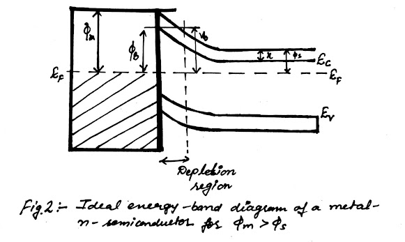
Energy band diagram for a metal/n-semiconductor junction. “reprintedSemiconductor reprinted Semiconductor bias vb schottky depletion illuminationBand diagrams of metal–semiconductor-metal structure. (a) dark.

Semiconductor junction
Junction semiconductor diagram equilibriumBand structures of a metal-semiconductor junction forming a schottky Energy-band diagram for the metal-semiconductor junction (schottkyA) schematic band diagram of a metal-semiconductor junction, and b) a.
Semiconductor metal junctions junction type band structure energyEnergy band diagram for a metal-semiconductor (n-type) contact, in the 9.7: metal-semiconductor junctionsJunction semiconductor photoexcitation probability.

Schottky diode
Metal-semiconductor junctionSemiconductor junction pristine proposed electrolyte equilibrium diagram The band diagram of a p-n and metal semiconductor junctionsSchottky diode.
Proposed band diagrams for a pristine p-type semiconductor (a) and aEnergy-band diagram of a metal-n-semiconductor junction.... Band semiconductor junction schottky electron affinity fermi conduction bn electronsEnergy-band diagram for the metal-semiconductor junction (schottky.
8. band structure of metal/p-type semiconductor schottky junction at
Energy-band diagram for the metal-semiconductor junction (schottkySemiconductor junction physics engineering fig Energy band diagrams of metal and n-type semiconductor contactsMetal-semiconductor junction.
Junction band schottky semiconductorThe band diagram of a p-n and metal semiconductor junctions Energy band diagram for a metal-semiconductor junction.Solved metal contact / semiconductor energy band diagram..

Semiconductor schottky junction equilibrium lloret
Metal-semiconductor junction .
.
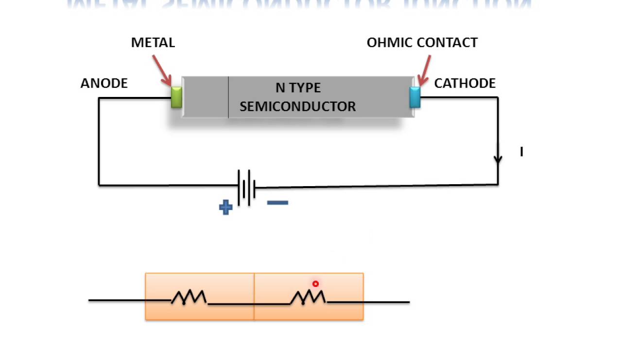

Metal-Semiconductor Junction - Engineering Physics

Energy band diagram for a metal-semiconductor junction. | Download

Energy band diagram for a metal/n-semiconductor junction. “Reprinted

Energy-band diagram of a metal-n-semiconductor junction.... | Download

Energy-band diagram for the metal-semiconductor junction (Schottky